数据布局说明
3 总体数据布局
ubi 方案FLASH 上的数据布局
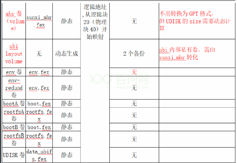
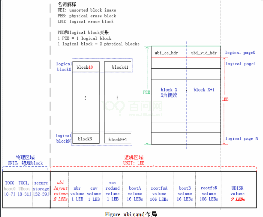
sys_partition.fex 文件中的各个分区大小会按照LEB 大小对齐,sunxi_mbr 分区概念与UBI卷(volume)概念相同 需要修改原镜像文件:物理区TOC0 合逻辑区sunxi_mbr.fex 需要动态生成文件:逻辑区ubi layout volume 注意:
- 各分区镜像以实际应用为准
- logical page0 = logical block 的两个page0
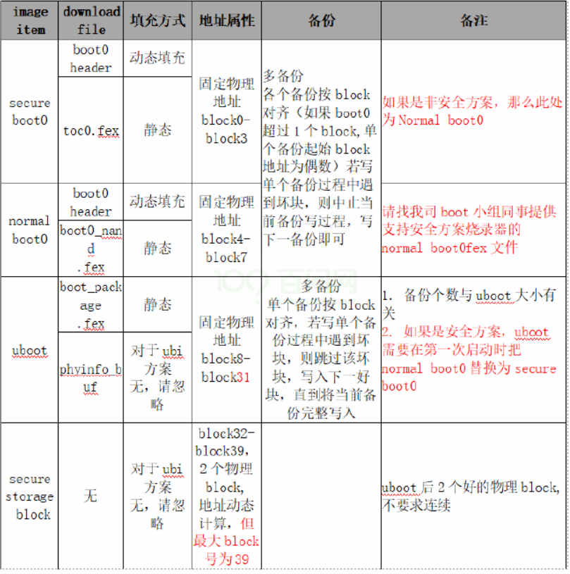
4 toc0 or boot0
4.1 input file
boot0_nand.fex(非安)or toc0.fex(安全)
4.2 flow
• 验证checksum 是否准确 • 填充storage_data • 重新生成checksum 并更新boot_file_head_t 中的check_sum
参考文件
include/private_boot0.h
sprite/sprite_download.c
参考函数
download_normal_boot0
download_secure_boot0
4.3 normal boot0
normal boot0 存放于block4-7 参考function: download_normal_boot0
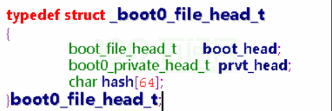
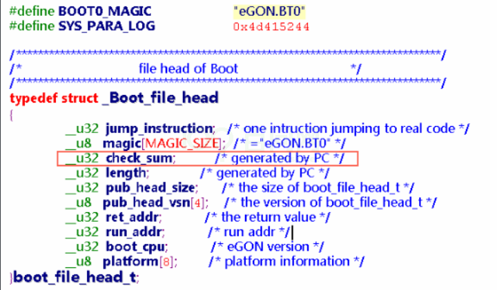
typedef struct _boot0_file_head_t
{
boot_file_head_t boot_head;
boot0_private_head_t prvt_head;
char hash[64];
__u8 reserved[8];
union {
#ifdef CFG_SUNXI_SELECT_DRAM_PARA
boot_extend_head_t extd_head;
#endif
fes_aide_info_t fes1_res_addr;
} fes_union_addr;
}boot0_file_head_t;
/******************************************************************************/
/* file head of Boot0 */
/******************************************************************************/
typedef struct _boot0_private_head_t
{
>-------__u32 prvt_head_size;
>-------/*debug_mode = 0 : do not print any message,debug_mode = 1 ,print debug message*/
>-------__u8 debug_mode;
>-------/*0:axp, 1: no axp */
>-------__u8 power_mode;
>-------__u8 reserve[2];
>-------/*DRAM patameters for initialising dram. Original values is arbitrary*/
>-------unsigned int dram_para[32];
>-------/*uart: num & uart pin*/
>-------__s32>-->------->------->------->------->-------uart_port;
>-------normal_gpio_cfg uart_ctrl[2];
>-------/* jtag: 1 : enable, 0 : disable */
>-------__s32 enable_jtag;
normal_gpio_cfg>---- jtag_gpio[5];
>-------/* nand/mmc pin*/
normal_gpio_cfg storage_gpio[32];
>-------/*reserve data*/
char storage_data[512 - sizeof(normal_gpio_cfg) * 32];
}boot0_private_head_t;
4.4 secure boot0
secure boot0 存放于boot0-block3
typedef struct sbrom_toc0_config
{
unsigned char config_vsn[4];
unsigned int dram_para[32]; // dram参数
int uart_port; // UART控制器编号
normal_gpio_cfg uart_ctrl[2]; // UART控制器GPIO
int enable_jtag; // JTAG使能
normal_gpio_cfg jtag_gpio[5]; // JTAG控制器GPIO
normal_gpio_cfg storage_gpio[50]; // 存储设备GPIO信息
// 0-23放nand,24-31存放卡0,32-39放卡2
// 40-49存放spi
char storage_data[384]; // 0-159,存储nand信息;160-255,存放卡信息
unsigned int secure_dram_mbytes; //
unsigned int drm_start_mbytes; //
unsigned int drm_size_mbytes; //
unsigned int boot_cpu; //
special_gpio_cfg a15_power_gpio; //the gpio config is to a15 extern power enable
gpio
unsigned int next_exe_pa;
unsigned int secure_without_OS; //secure boot without semelis
unsigned char debug_mode; //1:turn on printf; 0 :turn off printf
unsigned char power_mode; /* 0:axp , 1: dummy pmu */
unsigned char rotpk_flag;
unsigned char reserver[1];
unsigned int card_work_mode;
unsigned int res[2]; // 总共1024字节
}
sbrom_toc0_config_t;
4.5 filling storage_data
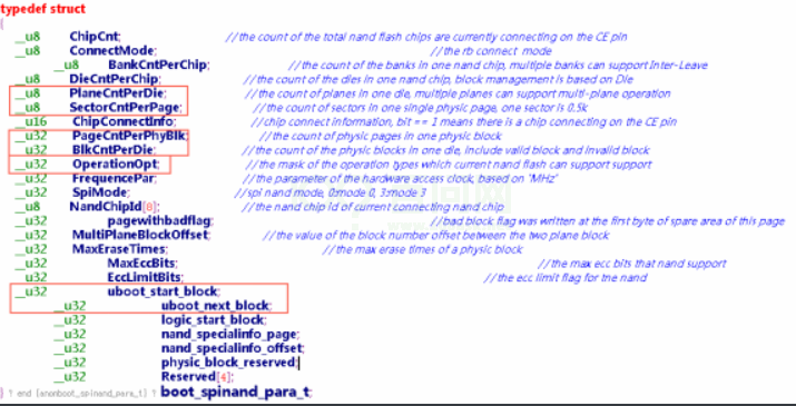
下表中红色字体不能配置错,大部分值直接参考drivers/mtd/awnand/spinand/physic/id.c
| attribute name | type | value | comment |
|---|---|---|---|
| ChipCnt | unsigned char | 1 | |
| ConnectMode | unsigned char | 1 | 忽略,可以不用理解 |
| BankCntPerChip | unsigned char | 1 | 忽略,可以不用理解 |
| DieCntPerChip | unsigned char | 1 | |
| PlaneCntPerDie | unsigned char | 2 | 忽略,可以不用理解 |
| SectorCntPerPage | unsigned char | 4 | 以具体物料为准, 常见为4 |
| ChipConnectInfo | unsigned short | 1 | 忽略,可以不用理解 |
| PageCntPerPhyBlk | unsigned int | 64 | 以具体物料为准, 常见为64 |
| BlkCntPerDie | unsigned int | 1024 | 以具体物料为准, 常见为1024,也可能为512 或2048 |
| OperationOpt | unsigned int | 0x? | 参考id.c 各个物料配置 |
| FrequencePar | unsigned int | 100 | 忽略,可以不用理解 |
| SpiMode | unsigned int | 0 | 忽略,可以不用理解 |
| NandChipId[8] | unsigned char | 0x? | 参考id.c 各个物料配置 |
| pagewithbadflag | unsigned int | 0 | 忽略,可以不用理解 |
| MultiPlaneBlockOffset | unsigned int | 1 | 忽略,可以不用理解 |
| MaxEraseTimes | unsigned int | 忽略,可以不用理解 | |
| EccLimitBits | unsigned int | 忽略,可以不用理解 | |
| uboot_start_block | unsigned int | 8 | |
| uboot_next_block | unsigned int | 40 | |
| logic_start_block | unsigned int | 40 | 忽略,可以不用理解 |
| nand_specialinfo_page | unsigned int | 0 | 忽略,可以不用理解 |
| nand_specialinfo_offset | unsigned int | 0 | 忽略,可以不用理解 |
| physic_block_reserved | unsigned int | 0 | 忽略,可以不用理解 |
| Reserved[4] | unsigned int | 0 | 忽略,可以不用理解 |
以GigaDevice GD5F1GQ4UBYIG spinand 为例,其大部分信息直接来自id.c
{
.Model = "GD5F1GQ4UBYIG",
.NandID = {0xc8, 0xd1, 0xff, 0xff, 0xff, 0xff, 0xff, 0xff},
.DieCntPerChip = 1,
.SectCntPerPage = 4,
.PageCntPerBlk = 64,
.BlkCntPerDie = 1024,
.OobSizePerPage = 64,
.OperationOpt = SPINAND_QUAD_READ | SPINAND_QUAD_PROGRAM |
SPINAND_DUAL_READ,
.MaxEraseTimes = 50000,
.EccFlag = HAS_EXT_ECC_SE01,
.EccType = BIT4_LIMIT5_TO_7_ERR8_LIMIT_12,
.EccProtectedType = SIZE16_OFF4_LEN8_OFF4,
.BadBlockFlag = BAD_BLK_FLAG_FRIST_1_PAGE,
},
参考文件:
include/linux/mtd/aw-spinand.h /定义id.c 中id 表的数据结构/
drivers/mtd/awnand/spinand/sunxi-spinand.h /定义boot_spinand_para_t 填充的数据结构/
drivers/mtd/awnand/spinand/sunxi-driver.c /填充函数参考/
drivers/mtd/awnand/spinand/physic/id.c /不同物料的信息配置(id 表配置)/
参考函数:
ubi_nand_get_flash_info–>spinand_mtd_get_flash_info
4.6 update checksum
参考文件:
sprite/sprite_download.c
sprite/sprite_verify.c
board/sunxi/board_common.c
参考函数流程:
download_normal_boot0/download_secure_boot0 -> sunxi_sprite_generate_checksum
-> sunxi_generate_checksum
4.7 burn boot0
注意事项: 如果是安全方案,存放boot0 的blocks 中一半存放secure boot0,一半存放normal boot0, 参考UBI 方案分区表信息以及第2 章节说明
各个备份按block 对齐(如果boot0 超过1 个block, 单个备份起始block 地址为偶数), 若写单个备份过程中遇到坏块,则中止当前备份写过程,写下一备份即可boot0 的镜像文件已经包含了boot0 header,不需额外分配组织boot0 header 格式,只需更新boot0 header 中的storage_data 部分,其他属性(比如dram_para)不需更新。更新后,需重新生成boot0 header 中的校验和check_sum
5 toc1 or uboot
区域:block8-block31 直接烧写toc1 镜像 参考文件:
sprite/sprite_download.c
drivers/sunxi_flash/nand.c
drivers/sunxi_flash/nand_for_ubi.c
drivers/mtd/awnand/spinand/sunxi-driver.c
参考函数:
sunxi_sprite_download_uboot–>sunxi_sprite_download_toc–sunxi_flash_nand_download_toc–>
ubi_nand_download_uboot–>spinand_mtd_download_uboot
6 secure storage block
区域:block32-block39 烧录器不用处理